Single-crystal silicon parts (wafers, targets, fabricated parts, etc.)
We stably supply high-quality single-crystal silicon parts. We also accept small-lot orders for prototyping, research, and other applications.
We supply silicon products processed in a range of shapes and surfaces to meet the needs of our customers, including silicon wafers (for research and development and for equipment testing and evaluation) and fabricated silicon products (routing, holing, cylinder fabrication).
Electronics
Features
We stably supply high-quality single-crystal silicon parts.
We also accept small-lot orders for prototyping, research, and other applications.
Silicon wafers for R&D and equipment testing/evaluation
- We supply high-quality wafers, including one-sided polished wafers 2 to 12 inches in diameter and wafers with oxide films.
- Following the needs of our customers, we are able to supply rectangular and non-OF (orientation flat) (round) wafers and also provide finishing processing, including double-sided polishing, double-sided etching, and double-sided lapping.
- We can manufacture wafers in thicknesses from 100 µm (4 inches) to 2000 µm.
Silicon wafers for sensors and MEMS
We supply high-precision wafers that support accurate groove fabrication for sensors and MEMS, which are depth etched.
- Smaller orientation tolerance (cutting angle)
- Smaller OF position angle tolerance
- Smaller thickness tolerance
- More precise flatness
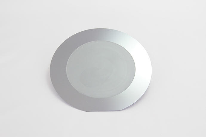
Sheets (materials for targets, etc.)
We supply silicon sheets for sputtering targets, which must have high precision, high purity, and high temperature characteristics, and for semiconductor-related manufacturing equipment, such as liquid crystal manufacturing equipment. We supply parts in the shapes and finishes requested by the customer.
Example shapes
- Shapes : Cylindrical, rectangular
- Chamfering : round chamfering, C chamfering, light chamfering
- Surface finish : mirror, etched, lapped, ground, sliced
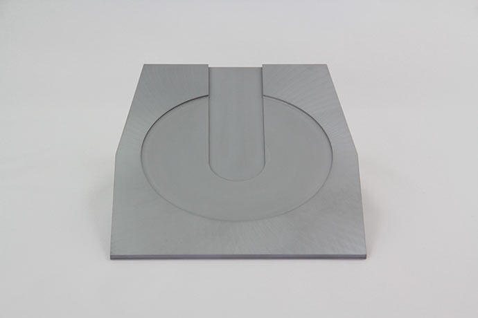
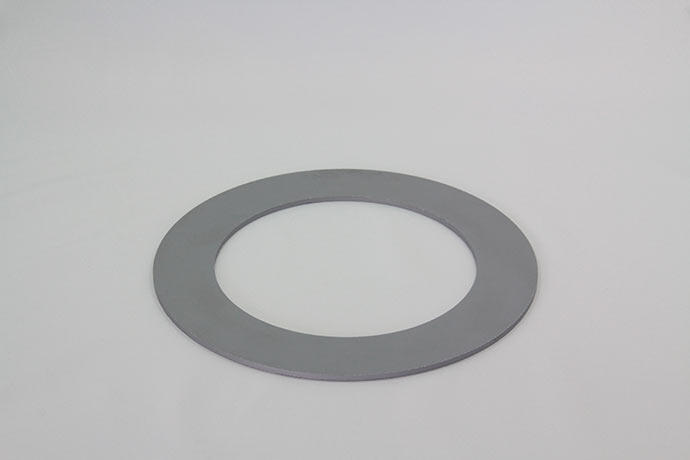
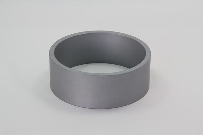
Special fabricated parts
We supply processed products in a range of shapes and surfaces to be used as high-purity material parts for many kinds of manufacturing equipment to meet the needs of our customers.
Processing example
- Male/female screw tapping
- Large/small ring fabrication
- Cylinder/prism fabrication
- Large/small holing
- Routing
- Slit fabrication
Applications
Silicon wafers for R&D and equipment testing/evaluation
- For R&D
- For testing and evaluating semiconductor equipment
- For evaluating resists and coating agents
- Substrates for film evaluation
Silicon wafers for sensors and MEMS
- For MEMS fabrication, such as waveguides and sensors
Sheets (materials for targets, etc.)
- For manufacturing liquid crystals
- For manufacturing touch panels
Special fabricated parts
- Parts for semiconductor manufacturing equipment
- Trays for wafer transport (routed parts)